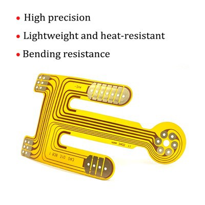
Stretchable PCBs are electronic circuits that have a thin substrate and conductive film respectively. This feature is widely used in modern electronic products and can replace traditional wire harnesses. Flexible printed circuits are bendable PCBs that directly connect electronic components, transmit electrical signals, and provide mechanical support. Flexible
What is lamination?
Lamination is one of the main steps in the manufacturing of flexible circuit boards. The so-called "lamination" is a method of ensuring that the flexible substrate, copper foil and cover layer are combined into a whole by lamination under certain conditions.
The lamination process mainly includes the following stages:
1. Material preparation and cleaning
Preparation of flexible substrates: Flexible substrates are usually made of polyimide or polyester. These materials have excellent mechanical properties and heat resistance.
Preparation of copper foils: Copper foils are used to form conductive wires. The thickness of the copper foil is selected according to the design needs.
Surface Cleaning: It is important to thoroughly clean the surfaces of the flexible substrate and the copper foil to remove dust, oil, grease, and other contaminants before bonding. Common cleaning methods include chemical and plasma cleaning.
Surface treatment: The copper foil is also subjected to a roughening process (e.g., chemical etching or mechanical roughening) to increase its surface area and thus improve bonding to the bonding layer.
2. Stacking of components
Stacking order: According to the design requirements, workers stack the flexible substrate, bonding layer (e.g. acrylic or epoxy) and copper foil in a specific order.
Alignment: It ensures that there is accurate alignment between the layers. Locating holes and alignment marks are usually used to prevent deviations during subsequent processing.
3. Hot pressing and pressurization
Laminator Setup: The assembled stack is placed into the laminator. The temperature and pressure parameters of the laminator are set to ensure that the process requirements are met.
Hot pressing process: Hot press at high temperature and high pressure. The hot pressing time is set according to the material and process requirements.
Curing of the adhesive layer: Under high temperature and pressure, the adhesive layer starts to soften and flow, and fills the gap between the copper foil and the flexible substrate. With the continuous action of temperature and pressure, the adhesive layer gradually solidifies to form a strong bond.
4. Cooling and post-processing
Cooling process: After lamination, the laminate must be cooled slowly to room temperature. Rapid cooling may result in internal stresses and warping of the material.
Removal of the laminate: Remove the cooled laminate from the laminator.
Inspection and post-processing: Inspect the laminate for quality assurance. Inspection items include bond strength, ply alignment, and cosmetic quality. Corrections and subsequent processing, such as drilling, copper cladding, and molding, are performed as necessary.
Lamination Process Precautions
In the process of laminating flexible circuit boards, several key points must be strictly controlled to ensure the quality and reliability of the final product:
1. Temperature Control
The temperature during the lamination process should be maintained at a constant level within the set range. The lamination temperature is typically around 180 °C. To obtain a uniform cure of the adhesive layer, ±5 °C is an acceptable deviation. Excessively high temperatures may cause thermal damage to the substrate and the adhesive layer, resulting in an impairment of the mechanical and electrical properties of the PCB, while temperatures that are too low may not allow the adhesive layer to cure completely, resulting in poor interlayer adhesion and consequently delamination or peeling.
2. Pressure Control
The pressure applied during the lamination process must be evenly distributed so that consistent adhesion is maintained throughout the stack. High pressures can cause deformation of the substrate, while low pressures may produce unevenly bonded layers.
Pressure range: Lamination pressures range from 100-200 psi. For example, high pressures may cause deformation of the substrate, especially wrinkles or thin flexible deformation. Too low a pressure may not allow the bonding layers to cure in full contact, resulting in insufficient bond strength and affecting the board's durability.
3. Lamination Time
Typically, lamination times vary from 30 minutes to 1 hour but must be precisely controlled according to material properties and technical requirements. If the lamination time exceeds the limit, it may lead to over-curing of the material, which may deteriorate its flexibility and electrical properties; too short a lamination time may lead to incomplete curing of the adhesive interface layer, resulting in insufficient bond strength and possible delamination during subsequent use. Therefore, to ensure that the adhesive has sufficient curing time, it is often necessary to monitor the curing profile of the adhesive to optimize the time setting.
4. Alignment technology
Accurate alignment between material layers is ensured by using high-precision positioning holes and alignment marks. Errors in alignment accuracy should be controlled to the micron level to ensure the functionality and performance of the circuit. Industry alignment errors are generally controlled to within ±0.1 mm with a limit of 0.075 mm. Alignment deviations can lead to circuit connection errors, affecting the functionality and performance of the board.
7 different types of finishes for PCBs and flexible PCBs
1. Electroless Nickel Immersion Gold (ENIG OR ENi/IAu)
Electroless Nickel Immersion Gold (ENIG) is a metallic coating used to improve solderability and prevent oxidation of copper contacts.
ENIG is a two-layer metal overlay with 2-8 μin nickel on top of 2-8 μin Au Ni at the top of 120-240 μin. It is usually applied by rapid immersion in a solution containing gold salts. The gold protects the nickel from oxidation, while the nickel protects and secures the base metal surface and allows circuits to be securely soldered to it. Due to RoHS regulations and developments, ENIG has become the most popular surface finish in the PCB industry.
Advantages: It does not oxidize easily, can be stored for long periods, has a flat and smooth surface, and is easy to solder to PCBs. Due to its thinness, it is more suitable for Stretchable PCBs for soldering precision pins, components, and small solder joints. The reflow process can be repeated many times without affecting solderability. It is RoHS-compliant and lead-free. Plated holes hold tighter tolerances.
Cons: Black pads can be a problem due to chemical nickel plating. Over time, the nickel layer oxidizes and long-term reliability is compromised.
2. Electroless Nickel Electroless Palladium Infusion Gold (ENEPIG).
ENEPIG was first introduced in the late 1990s and is relatively new to the board finishing market; ENEPIG is similar to ENIG. Palladium is used to protect the nickel layer and prevent it from oxidizing. ENEPIG is a good choice for applications that require high frequency and limited spacing. It is also compliant with packaging requirements and RoHS regulations. However, ENEPIG is not used as a surface treatment for printed circuit boards due to its high cost and low demand.
 3. Immersion Silver (ImAg)
Immersion tin is a metallic coating that is deposited and applied directly to the copper of a circuit board by a chemical displacement reaction.ISn protects the copper for its expected shelf life. The thickness of the immersion tin is typically between 20-50 μin. Interactions between tin, copper, and other metals will cause them to diffuse into each other. This will affect the shelf life of the coating and its performance. Immersion tin is suitable for small geometries and fine-pitch components. Immersion tin is less costly than ENIG or silver and is RoHS-compliant.
Advantages: Lead-free, RoHS compliant, and flat solder surface. Plated holes maintain tighter tolerances. Ideal for horizontal production. Precision wiring process.
Disadvantages: PCBs can be damaged and have soldering problems when handled. Tin whiskers are also a problem. Shorter shelf life than ENIG. Higher storage conditions. Contact switches are not properly designed. Solder masks have to be handled in a very strict manner or they will come off. For multiple soldering, it is advisable to use N2 gas. Electrical measurements can also be a problem.
5. Organic Solderability Preservatives (OSP)
OSP involves the chemical growth of a thin organic film on a clean, bare copper surface. This film is resistant to oxidation and thermal shock, as well as moisture to protect the copper from rusting. This protective film is not necessary in normal environments but is required for high-temperature soldering.
Advantages: Flat soldering surface, non-toxic and environmentally friendly, RoHS compliant. Less expensive than other surface treatments. Simple process for SMT and lead-free soldering.
Disadvantages: Limited reflow time, and poor resistance to high temperatures. Not suitable for lead bonding and crimping. Short soldering window, slightly lower long-term reliability. Not suitable for multiple soldering processes.
6. Electrolytic nickel/gold (hard/soft gold)
Electrolytic nickel/gold is a nickel base covered with a gold layer. The coating is categorized as hard gold (99.6% purity) or soft gold (99.9% purity). The type of application will determine whether you choose hard or soft gold.
Hard Gold Finishes
Hard gold is a gold alloy containing cobalt or nickel. Hard gold is a gold coating over a nickel layer. Low-stress nickel is used between the gold plating and the copper. Hard electrolytes consist of two layers: the gold plating and the nickel barrier. Hard gold is very durable and is well-suited for components with a high risk of wear, such as edge connectors, interconnect carriers, and contacts. It is not recommended for solderable areas due to its cost and poor solderability.
The thickness of hard gold finishes will vary depending on their application. If hard gold is used for military applications, the thickness must be between 50 and 100 μin. For non-military applications, a thickness of 25 to 50 μin is required.
Benefits: Lead-free, RoHS compliant, long shelf life. Storage life > 12 months. Ideal for electrical testing, contact switch design, and gold wire bonding.
Cons: Plating fingers with gold is very expensive and requires a special circuit to conduct electricity. Soldering can be difficult due to inconsistent gold thickness. Plating problems with uneven surfaces. Nickel-plated gold will not wrap around the edges of the wire.
Soft Gold Metallic Finish
Soft Gold finishes are gold finishes with a higher purity of gold in the outer layer. Soft Gold is 99.9% pure. Boards that require lead bonding and high solderability are often finished in soft gold. Soft gold produces stronger solder joints than hard gold.
In general, electrolytic nickel/gold finishes are the most expensive PCB finishes.
7. Hot Air Solder Leveling (HASL) / Lead-Free HASL
HASL or traditional surface preparation is a method of surface preparation. The board is immersed in a bath of molten solder to cover all surfaces exposed to the solder. The board is placed between hot air knives to remove any excess solder. The solder used in this case is a mixture of tin, lead, and zinc. the HASL method has an unexpected benefit: it exposes the PCB to temperatures up to 265°C, which allows any delamination to be detected before expensive components are attached. HASL makes the device more resistant to drops. the HASL method is the same as lead-free HASL. The only difference is that the solder is made from lead-free alloys such as tin-copper-nickel-germanium (T-Cu-Ni-Ge), tin-silver-copper (SAC), and tin-copper-cobalt (T-Cu-Co).HASL used to be the industry standard, but its popularity has declined due to possible RoHS compliance issues.
Pros: Low price, long shelf life, HASL can be reworked.
Cons: Uneven solder surface, contains lead (not RoHS compliant), can't hold tight tolerances on plated holes.
Group Profile
ZHUHE Group is a comprehensive service provider of electronic technology and electronic products for more than 10 years. Starting from a small company, we have continued to expand the field of electronic applications and provide customers with advanced intelligent control solutions, and have grown to have 11 subsidiaries of our own. We can provide professional OEM/ODM service to our customers. The company is well-managed and insists on providing quality products and services to customers.

The Group has diversified products and technologies, including semiconductor devices, pulse motors, high frequency transformers, inductors and PCBA (Printed Circuit Board Assemblies) and FPCA (Flexible Printed Circuit Assemblies), which are the core components of a variety of electronic products, and specializes in the fields of high-speed data transmission and communications, automotive electronics, medical electronics, industrial control products and new energy technologies. Currently, our main markets are domestic and overseas.

We can provide customers with single and double-sided boards, high and multi-layer boards, soft and hard combination boards, special process flexible boards, etc.; we can also customize the products that customers need according to the drawings or samples provided by customers. We strictly control the product quality in every step of the manufacturing process and provide leading technical support. Before cooperation, we will have a professional technical team to answer your questions. During the cooperation, we have specialized technical team for you. After cooperation, we have specialized technicians to serve you one to one.

Q: What is the difference between flexible circuit board and rigid circuit board?
A: The biggest difference between flexible circuit boards and rigid circuit boards is their bendability. Flexible circuit boards can be bent or folded as they operate, allowing for precision connections in places that were not even imagined. Rigid circuit boards, on the other hand, do not have such bendability.
Q: What are the main applications of flexible circuit boards?
A: At present, flexible circuit boards have been widely used in wearable electronic devices, folding smartphones, automotive electronics, drones, and other fields, these products need to design very complex circuits and need to go through repeated bending and folding, so flexible circuit boards play a key role. And many application scenarios are still being explored.
Q: What are the advantages of Stretchable PCBs?
A: The flexible circuit board has a lot of advantages, it can adapt to a variety of complex shape designs, increase the design flexibility of the product, it can also reduce the size of electronic products, making them more light and carriable, so that the flexible circuit board becomes a highly coordinated function and shape of the electronic product realization mode, and it has the characteristics of saving resources, low manufacturing cost and lightweight. In conclusion, flexible circuit boards are used in a wide range of applications and have many unique technical advantages.
Hot Tags: stretchable pcb, China stretchable pcb manufacturers, suppliers, factory, Flexible Printed Circuit Board, Bipolar Junction Transistor Bjt, , IRF250N Mosfet, Flexible Fpc, Flexible Printed Board