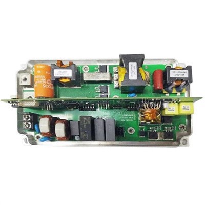
PCB assembly components refer to the process of soldering electronic components (such as capacitors, resistors, chips, etc.) to a printed circuit board to form a complete circuit board system. PCBA contains a number of important components, the core of which is the printed circuit board (PCB).
PCB is a plate-like substrate made of insulating materials on which a special process is used to form circuit patterns such as wires, component mounting positions, etc. The design and production of PCB are the foundation of PCBA, and reasonable layout and accurate production determine the performance and reliability of PCBA.
There are four main links in the PCBA production process
In terms of technology, the process of PCBA can be roughly divided into four main links, namely: SMT chip processing, DIP plug-in processing, PCBA testing, and finished product assembly.

1. SMT chip processing link
In the SMT chip processing process, the components will be matched and purchased according to the BOM matching list provided by the customer, and the PMC plan of production will be confirmed. After the preparatory work is completed, SMT programming begins, a laser stencil is made according to the SMT process, and solder paste printing is performed.
With the SMT placement machine, the components are mounted onto the circuit board, and in-line AOI automatic optical inspection is performed if necessary. After testing, set the perfect reflow oven temperature profile to allow the board to flow through the reflow soldering.
After the necessary IPQC inspection, the DIP plug-in process is used to pass the plug-in material through the circuit board and then flow through wave soldering for soldering. This is followed by the necessary post-furnace process.
After the above processes are completed, QA will conduct a comprehensive inspection to ensure that the product quality is satisfactory.
2. DIP plug-in processing link
The process of DIP plug-in processing is: plug-in → wave soldering→ shearing → post-welding→ washing → quality inspection
3. PCBA test
PCBA testing, the most critical quality control link in the entire PCBA process, needs to strictly follow the PCBA test standards and test the test points of the circuit board according to the customer's test plan.
PCBA testing also includes 5 main forms: ICT testing, FCT testing, aging testing, fatigue testing, and testing in harsh environments.
4. The finished product assembly
The PCBA board that is OK for testing is assembled for the housing, then tested, and finally it is ready to be shipped.
PCBA production is a link to a link; any link that has a problem will have a very big impact on the overall quality, and each process needs to be strictly controlled.
The above is about the four main links of PCBA process production; each big link has countless small links to assist, and each small link will have one or some test processes to ensure product quality and avoid the outflow of unqualified products.
Why PCB circuit boards need to do test points?
I. Reasons for Testing Printed Circuit Boards
Basically, the purpose of setting up checkpoints is to check whether the components on the circuit board meet the specifications and characteristics. For example, if you want to check if there is a problem with the resistance on the circuit board, the easiest way is to measure it using a multimeter. You can find out the answer by measuring both ends.
However, in a mass-production factory, there is no way to slowly measure the correct circuitry of every resistor, capacitor, inductor or even IC on every board of a printed circuit board with a meter.
Hence the emergence of so-called ICT automated inspection machines, which use multiple probes to contact all the part lines on the board that need to be measured, and then are programmed to measure these electronic components in turn, on a sequence basis and in a side-by-side manner. Properties of the parts.
Typically, completing an inspection of all parts of a printed circuit board in this manner takes only about 1 to 2 minutes, depending on the number of parts on the board. The more parts, the longer it takes.
However, assuming that these probes are in direct contact with the electronic components on the board or their solder pins, it is likely that they will crush some of the electronic components, but it would be counterproductive.
 So, a clever engineer made a clear "checkpoint", and a pair of dots on both ends of the part. There is no soldermask (mask), so the probe can be used to check these dots, without direct contact with those being measured by the electronic components of the printed circuit board.
In the early days of circuit boards, or the traditional plug-in (DIP) era, the solder pins of the parts were indeed used as inspection points, because the solder pins of traditional parts are strong enough not to be afraid of pin-prick, but often the probe. Misjudgment of poor contact occurs.
Since electronic parts are generally wave soldered or SMT tinned, a film of solder paste flux residue usually forms on the surface of the printed circuit board solder. This film has a very high impedance and usually constitutes a probe. Contact is poor, so it is common to see inspection operators on the production line desperately blowing with air guns or wiping the panel to be inspected with alcohol.
However, as technology advances, circuit boards are getting smaller and smaller. It has become a bit of a struggle to squeeze so many electronic parts onto a small circuit board. As a result, the problem of checkpoints taking up space on the board is often planned. A tug-of-war between the terminals and the manufacturing terminals.
Checkpoints generally have a rounded appearance because the probes are also round, which makes them easier to fabricate and simpler to bring neighboring probes close to each other so that the needle density of the needle bed can be increased.
II. Reasons for using a needle bed for printed circuit board inspection
1. Using a needle bed for circuit inspection imposes some inherent constraints on the mechanism. For example, there is a limit to the minimum diameter of the probes; needles with too small a diameter can easily break and be damaged.
2. there is also a degree of constraint on the distance between pins because each pin must exit a circuit board hole and a flat cable must be soldered to the back end of each pin, assuming that the adjacent holes are too small, in addition to the problem of shorting contacts between pins, and flat cable intervention is a major problem.
3. Some high places cannot be inserted with pins. Assuming that the probe is too close to a high part, there is a risk of hitting the high part and causing damage. In addition, due to the high parts, holes should be punched in the needle bed holder of the inspection tool to avoid this, which directly means that no needles can be implanted. It is becoming increasingly difficult to accommodate checkpoints for everything underground on the board.
4. The number of checkpoints has been commented on repeatedly as boards get smaller and smaller. There are now ways to reduce the number of checkpoints and other tests that want to replace the original pin bed test. There does not seem to be a test that is a 100% replacement for ICT.
Group Profile
ZHUHE Group is a full-service EMS service provider, providing high-quality electronic manufacturing solutions to customers in the industry. Relying on stable and high-quality manufacturing capacity, the company takes R&D as the core driving force to provide customers with one-stop services in the true sense of design, procurement, manufacturing, etc., build a complete PCBA ecological chain, and ultimately realize the company's overall product competitive advantage.

In terms of processing and manufacturing, ZHUHE Group is able to realize the whole process of PCBA automatic production and manufacturing of finished electronic products. In addition, the company is also able to provide customers with BGA, CSP, POP and other complex packaging device repair services. These high-quality services provide customers with a full range of full-process electronic manufacturing solutions to meet the different needs of customers in the industry.

As a technology-led enterprise, Zhuhe Group has always been market-oriented and technological innovation as its purpose. The company not only has strong capabilities in manufacturing, but also has very strong strength in research and development. Through its own strong R&D strength, the Group continues to introduce innovative solutions for electronic products and continuously promote the development of the entire industry.
In the process of enterprise development, Zhuhe Group has always adhered to the mission of creating a safe, efficient, and portable backup power supply. As one of the leading enterprises in the solar backup power industry, the company actively promotes the application of green energy and has made positive contributions to social development.

Q: What is printed circuit board assembly?
A: PCB assembly components is to solder electronic components (such as resistors, capacitors, chips, etc.) to the printed circuit board according to a specific layout, and connect them into a complete circuit system to play a specific function.
Q: What are the usually parts of PCBA products?
A: PCBA products are typically composed of printed circuit boards, components, soldering, assembly and testing. Among them, components include resistors, capacitors, chips, transistors, and so on. The welding methods typically include plug-in welding, surface welding and single-sided lead welding.
Q: What are the benefits of printed circuit board assembly?
A: The advantage of printed circuit board assembly is that it can greatly reduce the size and weight of the circuit system, improve the reliability and stability of the circuit system, and at the same time, it can also greatly reduce the manufacturing cost of the product.
Hot Tags: pcb assembly components, China pcb assembly components manufacturers, suppliers, factory, Large PCB Board, , , Advanced Circuits PCB, IRF250N Mosfet