
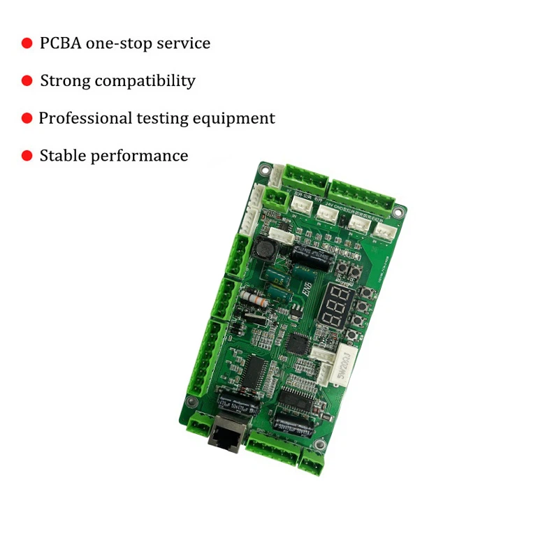


PCB ASM, or Printed Circuit Board Assembly, is the process of mounting electronic components onto a PCB to create a functional electronic circuit. The process involves multiple stages, including component sourcing, placement, soldering, and testing. The result is a fully assembled board that can be integrated into an electronic device.
PCB Design and Prototyping
The journey of a PCB begins with its design. Engineers use specialized software to lay out the circuit schematic and determine component placement and route alignment. This design undergoes rigorous testing and simulation to ensure functionality and reliability.
PCB prototyping follows the design phase where a small batch of PCBs is fabricated to validate the design. Prototyping allows engineers to detect and resolve any issues before mass production.
PCB design and prototyping involve several key steps to ensure a successful outcome. Here is a structured approach you can follow:
1. Define requirements and specifications
- Function: Clearly define what the PCB needs to do.
- Constraints: Consider dimensions, power requirements, environmental conditions, etc.
- Components: List all components and their specifications.
2. Schematic Design
- Use schematic capture software (e.g. Eagle, KiCad, Altium Designer) to create the circuit diagram.
- Ensure that all components are properly connected as required.
3. PCB Layout Design
- Transfer the schematic to a PCB layout tool.
- Place components strategically to minimize noise, optimize signal integrity, and ensure proper heat dissipation.
- Carefully route components to avoid signal interference and ensure manufacturability. 4.
4. Design Rule Check (DRC)
- Design Rule Checks (DRC) are run to ensure that the layout meets manufacturability and constraints (e.g., minimum alignment widths, clearances, etc.).
5. Prototyping
- Generate Gerber files (standard PCB manufacturing files) from your PCB layout software.
- Select a PCB manufacturer that meets your quality, turnaround time, and cost requirements.
Submit the Gerber file for manufacturing.
PCB Manufacturing Process
1. Substrate Preparation: Preparation and cleaning of the substrate material, usually fiberglass (FR4) or similar, to ensure that it is free of contaminants that could affect the performance of the PCB.
2. Copper Cladding: A thin layer of copper foil is bonded to the substrate through a combination of heat and adhesives. This copper layer will form the conductive traces and pads of the PCB ASM.
3. Photoresist application: A layer of photoresist material is applied to the copper-clad substrate. This photoresist is sensitive to light and protects certain areas of the copper from being etched away in the next step.
4. PCB Etching: The PCB is exposed to a chemical solution that removes the unprotected copper, leaving behind the alignments and pads defined by the photoresist pattern. The remaining photoresist is then peeled off to expose the copper traces.
5. PCB Drilling: A precision drill creates holes called through holes in the PCB where components will be mounted and where different layers of the PCB need to be electrically connected.
6. PCB Plating: Through holes and sometimes the entire surface of the PCB is plated with a thin layer of conductive material, usually copper, to ensure electrical continuity and enhance the durability of the PCB.
7. Screen Printing: Ink is applied to the surface of the PCB using a process similar to screen printing to mark component outlines, reference marks, test points, and other information.
PCB Assembly Process
After the bare PCB is manufactured, it enters the assembly process:
1. Component placement: Automated machines or technicians use placement machines to place surface-mounted components (SMDs) onto the PCB. Through-hole components are manually inserted into pre-drilled holes or using automated insertion equipment.
2. Soldering: Soldering components to the PCB to create electrical connections. This can be accomplished using wave soldering (for through-hole components) or reflow soldering (for SMDs), where solder paste is applied to the pads before placing the component and then heated to melt the solder.
3. Inspection and Testing: Automated Optical Inspection (AOI) machines check for solder defects, component placement accuracy, and potential shorts or opens. Functional testing ensures that the PCB operates as intended.
4. Forming: PCBs may be cleaned after testing to remove flux residue and other contaminants. They are then separated from the panel where multiple PCBs are fabricated together and may receive additional coatings for protection or aesthetics.
What are the causes of PCB voids in SMT processing?
 First of all, we need to understand the process of SMT processing.SMT (Surface Mount Technology) is a method of mounting electronic components directly onto the surface of a printed circuit board. The technology has the advantages of simple structure, small size, fast signal transmission rate, etc. It has become the main way of modern electronic manufacturing.
In SMT processing, the generation of PCB voids is mainly related to the mounting process. SMD process generally includes three steps: unloading, mounting, and soldering.
Step 1: Unloading. In SMD processing, the need to use automatic unloading machine components from the material tray, due to the material surface adsorption of air dust and other impurities, thus leaving a large number of tiny air holes in the material surface.
Step 2: Mounting. During the mounting process, the component is clamped by a positioning device and moved to a predetermined position after being positioned. However, due to the presence of tiny air holes on the surface of the component, when the component comes into contact with the PCB surface, the air between it and the PCB surface is squeezed out and holes are formed.
Step 3: Soldering. During the soldering process, the hole is further heated, and under the action of the brazing material, the metal between the brazing material and the PCB pads is melted, and the component is soldered to the PCB surface.
In short, in the process of SMT processing, the generation of voids is mainly due to the presence of tiny air holes on the surface of the component, when the component is in contact with the PCB surface, the air between it and the PCB surface is squeezed out, forming voids.
There are other reasons for PCB voids:
- Insufficient flux activation:
Voids form when the flux (a chemical used for soldering) is not sufficiently activated. The flux is critical to removing oxides and promoting proper wetting of the solder to the surfaces being joined.
- Captured Volatiles:
Certain materials, such as moisture or solvents, may become trapped in the solder paste. During the soldering process, these materials become gaseous and create voids in the solder joint.
- Insufficient preheating:
Inconsistent preheating of the PCB and components can cause the volatiles in the solder paste to evaporate quickly, creating voids.
- Incorrect solder paste composition:
The composition of the solder paste, including the type and size of the solder particles, can affect the formation of voids. Using the wrong solder paste for a particular application may increase the likelihood of voids.
What are the effects of PCB voids?
- Reduced mechanical strength:
Voids can affect the mechanical strength of solder joints. The presence of air pockets can weaken the bond between the component and the PCB, leading to potential joint failure under mechanical stress.
- Reduced thermal performance:
Air voids act as insulators and reduce the thermal conductivity of the solder joint. This can affect the component's ability to dissipate heat and may lead to overheating issues.
- Electrical Performance Issues:
Voids may alter the electrical characteristics of the solder joint, affecting conductivity and potentially leading to electrical failures or intermittent connections.
How do I avoid PCB voids?
To avoid PCB voids, the first step is to keep the SMD processing site clean and sanitary. Avoid dust, grease, fingerprints, and other pollutants in the unloading and installation process, and at the same time choose good quality, smooth surface, components without air holes in the parts.
In addition, a vacuum suction port or handling suction port can be used to reduce the pollution of the component surface and the air atmospheric experiments on the impact of air hole extrusion. At the same time, in the placement process to maintain the appropriate regulation of the pressure and temperature of the board can also effectively avoid the generation of voids.
PCB voids, although a common problem, but as long as attention is paid to a variety of details in the patch processing process, you can effectively avoid its generation, to ensure the quality and reliability of the patch processing.
Addressing and preventing voids in PCB solder joints requires a holistic approach that includes careful consideration of materials, process parameters, and equipment. Continuous improvement and adherence to industry standards can help minimize voids and ensure the reliability of electronic assemblies.
What is the PCB component placement process?
1. Design for Assembly (DFA)
Before physical assembly can begin, PCB layout and design must consider the principles of DFA:
- Component Orientation: Optimize orientation for ease of assembly and efficient routing.
- Gaps and Spacing: Ensure adequate soldering space and avoid interference between components.
- Accessibility: Facilitates automated or manual assembly processes.
2. Automated component placement
Modern PCB assembly often involves automated pick and place machines:
- Vision systems: Cameras recognize datum marks or component outlines on the PCB to accurately align and place components.
- Component Feeding: Components are loaded into a feeder and the feeder supplies them to the pick and place machine.
- Pick and Place Process: The machine uses vacuum nozzles to pick up components from the feeder, accurately aligns them to the corresponding pads on the PCB, and then gently places them using controlled motion.
3. Manual component placement
For specialized components or small batch production, manual placement can be used:
- Skill and precision: Technicians use hand tools such as tweezers and magnifiers to accurately place components.
- Prototype builds: Initial prototypes or small batches may benefit from manual placement for flexibility and customization.
What should I consider when placing components on a PCB?
Component placement is more than just arranging components on a board; it involves strategic decisions that affect the overall function and quality of the PCB. Proper placement not only ensures proper circuit operation, but also affects signal integrity, thermal management, and ease of assembly. Here are some key aspects to consider:
1. Signal Integrity Design
Signal integrity is critical to the proper operation of high-speed digital and sensitive analog circuits. To maintain signal integrity:
- Minimize Alignment Length: Minimize alignment length by placing critical components closer together to reduce signal delay and electromagnetic interference (EMI).
- Signal Path: Follow the logical signal flow from inputs to outputs and avoid crossing high-speed signals with noisy or high-current alignments.
- Grounding: Ensure robust grounding layers and strategically ground components that require low impedance connections to minimize noise and ground loops.
2. Thermal Management
Certain components, such as power transistors or voltage regulators, generate heat during operation. Efficient thermal management is essential to prevent overheating and ensure reliability:
- Heat sinks: Provide adequate space and mounting locations for heat sinks or thermal pads.
- Airflow: Arrange components to allow natural or forced airflow through the heat-generating components.
- Isolation: Prevent thermal damage by keeping heat-sensitive components away from components that generate a lot of heat.
3. Manufacturability and Assembly
Designing for manufacturability includes ensuring that PCBs can be assembled efficiently with minimal errors and rework:
- Component accessibility: Ensure that components are placed in such a way that they can be easily soldered by manual or automated pick-and-place machines.
- Orientation: Consistently align components to facilitate assembly and avoid errors during soldering.
- Clearance and Spacing: Adhere to manufacturing guidelines for minimum clearances between components to ensure that soldering and inspection can be accomplished smoothly.
4. Electromagnetic Compatibility (EMC)
PCB layout plays a critical role in achieving EMC compliance by reducing EMI emissions and susceptibility:
- Component Alignment: Position sensitive components and alignments to minimize loop areas and coupling.
- Shielding: Grouping and shielding sensitive components from noise sources such as high current paths or switched circuits.
- Grounding and routing: Properly routing and grounding signal return paths to minimize loop area and impedance discontinuities.
Group Profile
ZHUHE Group has been a comprehensive service provider of electronic technology and electronic products for more than 10 years. Starting from a small company, we have continued to expand the field of electronic applications and provide customers with advanced intelligent control solutions, and have grown to have 11 subsidiaries of our own. We can provide professional OEM/ODM service to our customers. The company's management is standardized and insists on providing customers with high-quality products and services.

ZHUHE upholds the spirit of independent innovation to continue to deepen the ODM business, to develop the new energy vehicle market, to provide strong technical support for the development of the industry by strong innovation capabilities, and the whole industry chain synergistic innovation, new energy projects to provide planning and design, technical support, engineering and construction, intelligent operation, such as integrated, one-stop services, to provide the industry with a solid strength of patented technology to provide professional services and excellent We provide professional services and excellent products for the industry with solid strength of patented technology.

The company takes R&D as the core driving force, through its strong R&D strength, relying on stable, high-quality manufacturing capacity, to complete the "one-stop" service for customers in the true sense of the word, including design, procurement, manufacturing, etc., to build a complete PCBA ecological chain, and ultimately to realize the company's overall product competitive advantage.

Q: What are the common problems in the PCB assembly process?
A: Common issues in PCB assembly include wrong component polarity, short circuits, missing or damaged solder joints, insufficient component clearance, reverse mounting, overheating of pads, etc. These issues can lead to component failure, unstable product performance, or circuit failure.
Q: What are the advantages of PCB ASM?
A: PCB assembly enables fast, efficient, accurate, and consistent assembly, reducing the risk of human error. Compared with manual assembly, machine assembly can improve production efficiency and quality, and it is more economical.
Q: What problems should be paid attention to in the assembly of PCBA?
A: The assembly of PCBA needs to pay attention to anti-static, moisture-proof, dust-proof, anti-vibration, and other issues. In the assembly process, it is necessary to arrange reasonably according to the actual situation to avoid problems such as errors and missing installations of components.
Hot Tags: pcb asm, China pcb asm manufacturers, suppliers, factory, Filter Coil Inductor, Power Supply, Huawei Phone Wireless Charger, Samsung Mobile Phone Wireless Charger, Advanced Circuits PCB, Home EV Charger


